The bending details

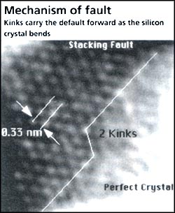
that the shape of a material can be distorted by applying sufficient force is well known. What is not very clearly understood are the processes going on at the atomic level which take place, when for instance, a piece of metal is bent. But now a group of scientists have reported seeing the initialisation of the process of bending in a silicon wafer.
John Spence and his team from the Arizona State University in Tempe, us, and the University of Koln, Germany, have captured the first images of atomic
